Characterization Capabilities
01: In situ Heating and Gas TEM 02: In situ Liquid TEM 03: Structure and Morphology Determination (HRTEM, SAED, sub-Å STEM) 04: Elemental Mapping and Composition (EDXS) 05: Chemical State/Bonding (EELS) 06: 3D Structure and Composition (Electron Tomography) 07: Nanoscale TEM Orientation and Phase Mapping (SPED/ACOM/ASTAR) 08: Quantitative Mass Measurement (Quantitative STEM) 09: Surface Topography (SEM) 10: Ex situ Gas Reactor01: In situ Heating and Gas TEM
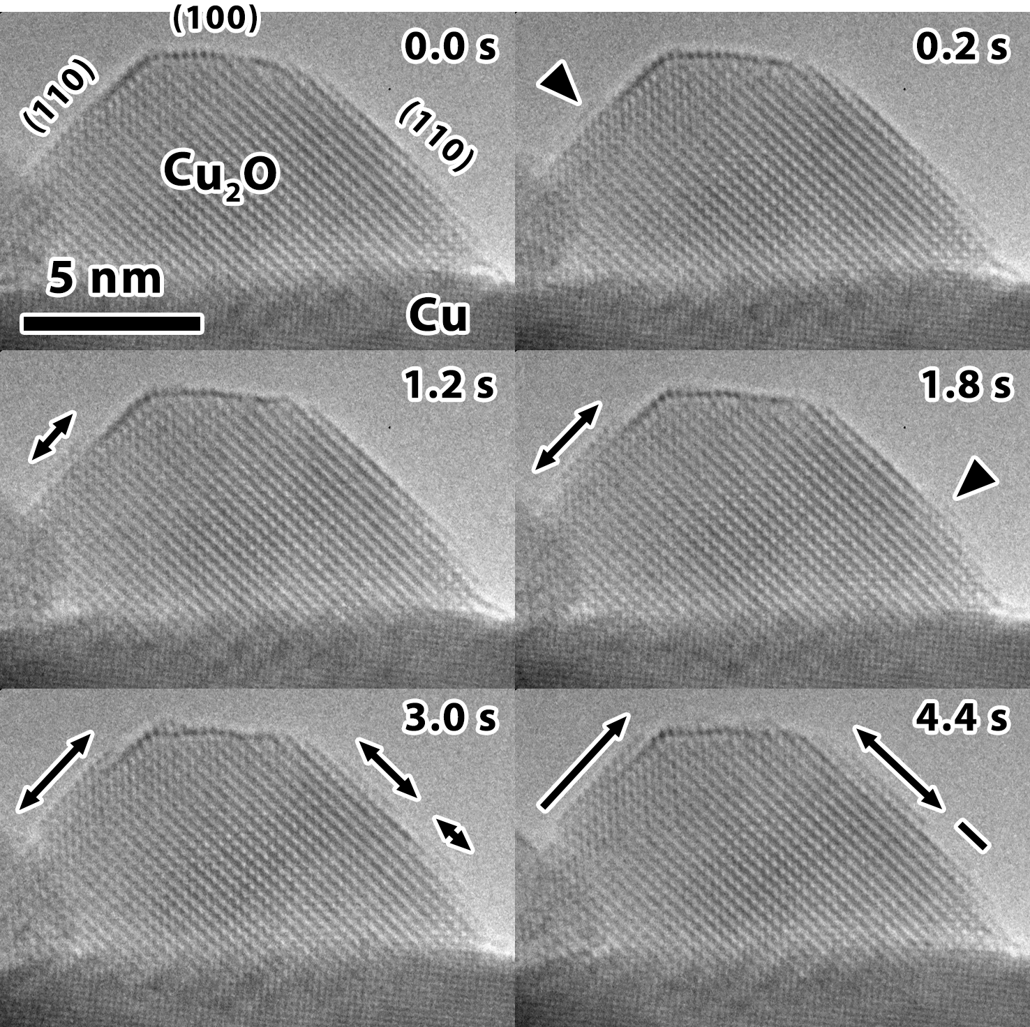
The Hitachi H-9500 ETEM is equipped with a custom-built, computer-controllable gas manifold system that supports the precise delivery of up to two gases and one vapor, at pressures up to 10-2 Pa. Specialized heating holders enable samples to be heated (with or without gas) up to 900 °C. The ECC has two styles of heating holder, enabling both thin film (“bulk”) and nanoparticle (supported on a membrane) specimens to be examined. High-resolution in situ imaging can be acquired at speeds up to 25 frames-per-second.
Currently attached gas sources include H2, O2, CO, CO2, CH3OH, and CH4; this selection can be easily expanded.
An example of this ETEM being used to study the early stages of Cu oxidation at the atomic scale can be found here: Li, M., Curnan, M.T., Gresh-Sill, M.A. et al. Unusual layer-by-layer growth of epitaxial oxide islands during Cu oxidation. Nat Commun12, 2781 (2021). https://doi.org/10.1038/s41467-021-23043-w
Figure: Layer-by-layer growth of Cu2O island on Cu (copper oxidation).
02: In situ Liquid TEM
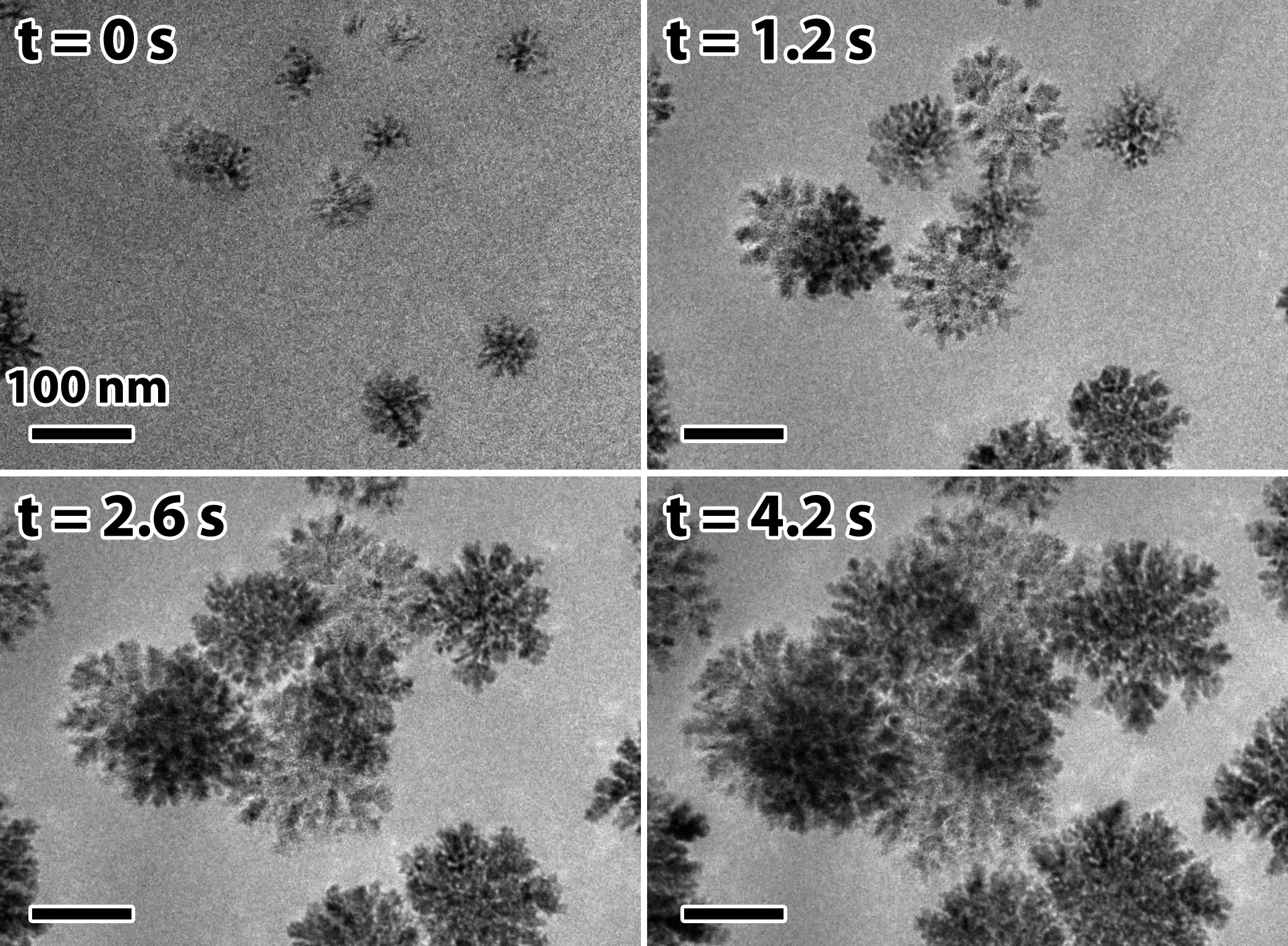
A specialized, closed-cell sample holder enables specimens in solution to be examined using TEM. This capability is crucial for the study of materials intended for use in liquid environments or liquid phase reactions. This includes particle nucleation and growth or tracking particle movement.
The liquid flow holder is compatible with the Hitachi H-9500 ETEM.
Figure: In-liquid growth of dendritic carbon nanoparticles.
03: Structure and Morphology Determination (HRTEM, SAED, sub-Å STEM)
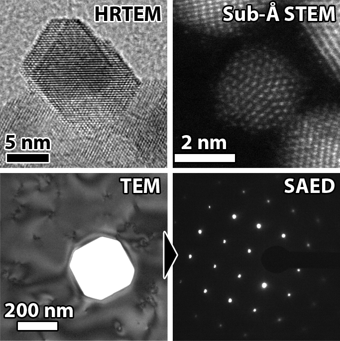
TEM offers a powerful range of different characterization modes for determining the crystal structure, orientation, size, and morphology of materials from the micrometer- to angstrom-scale. This includes identifying the exposed facets, defects, and surface reconstructions present in catalyst materials. Such characterization can be performed in situ at up to 25 frames-per-second, for following the evolution of the structure and morphology during reaction.
| Microscope | HRTEM | Sub-nm STEM | Sub-Å STEM | SAED | CBED |
| Hitachi H-9500 | x | x | ~ | ||
| JEOL 2100F | x | x | x | x | |
| FEI Themis | x | x | x | x | x |
04: Elemental Mapping and Composition (EDXS)
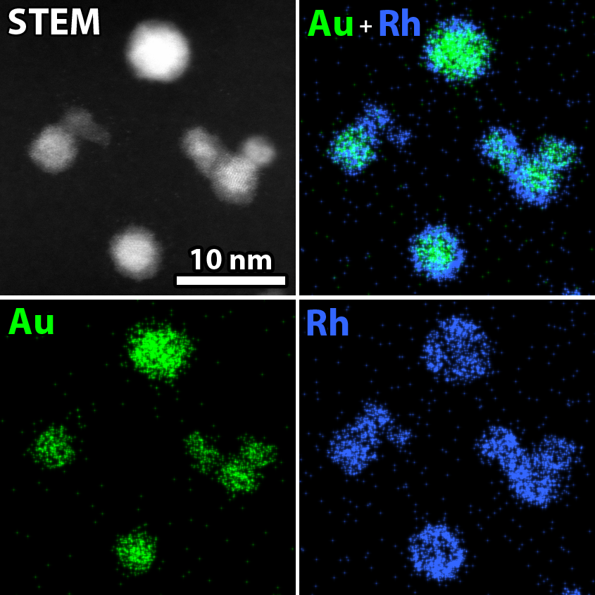
Energy-Dispersive X-ray Spectroscopy (EDXS) enables the quantification of elemental composition and even mapping of each element’s spatial distribution. Elements with Z ≥ 4 (Be and heavier) can be detected. Example applications include determining whether a bimetallic nanoparticle is a random alloy, core-shell, Janus-like, etc, or determining the uniformity of a batch of synthesized catalyst.
The FEI Themis 200, in particular, is equipped with a state-of-the-art Super-X quad-EDXS detector with field-leading speed and sensitivity.
Instruments equipped for EDXS:
| Microscope | EDXS Capabilities | Notes |
| Hitachi H-9500 | Area-composition | Down to 50 nm areas |
| JEOL 2100F | Point, line, mapping | Can determine composition of single nanoparticles down to 5-10 nm in size |
| FEI Themis | Point, line, mapping, 3D EDXS tomography | Can map distribution of elements inside particles down to 1-2 nm in size |
05: Chemical State/Bonding (EELS)
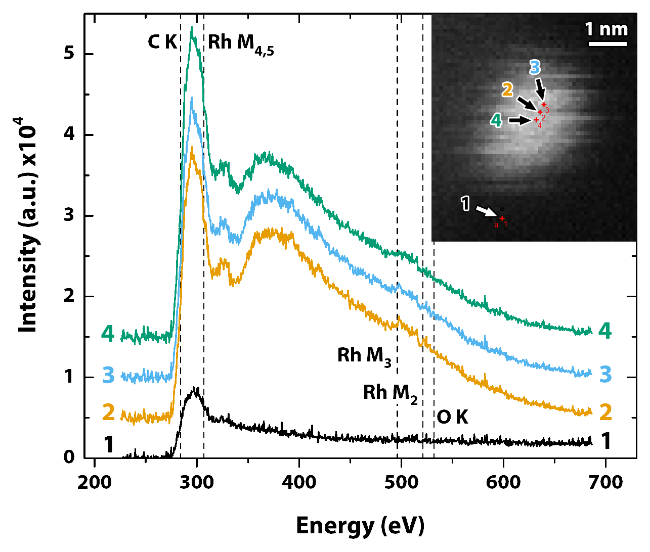
Electron Energy-Loss Spectroscopy (EELS) allows the direct investigation of local (nano-scale) chemistry and electronic structure of a material. EELS can be used, for example, to determine the oxidation state of a metal particle and (if large enough) whether this spatially varies.
The JEOL JEM-2100F is equipped with an EELS system.
Figure: EELS spectra confirming no significant oxidation of Rh nanocluster catalyst.
06: 3D Structure and Composition (Electron Tomography)
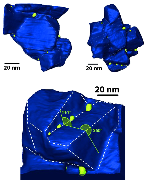
Analogous to a medical CAT scan, but using electrons instead of X-rays, electron tomography enables the acquisition of true, three-dimensional nanometer-resolution reconstructions of internal and external specimen structure. The sensitivity of the specimen to the extended electron doses required by electron tomography is typically the limiting factor to whether these techniques can be applied to a given material system. Example applications include determining the 3D morphology and dispersion of catalyst nanoparticles inside the host material, mapping the 3D pore network of a material, or creating 3D elemental distribution maps of a sample.
The FEI Themis G2 200 will be capable of electron and EDXS tomography.
Figure of tomographic reconstruction Au nanoparticles on mixed oxide support catalyst adapted from Gonzalez et al., Angew Chem Int Ed, 2009, 48, pp. 5313-5315.
07: Nanoscale TEM Orientation and Phase Mapping (SPED/ACOM/ASTAR)
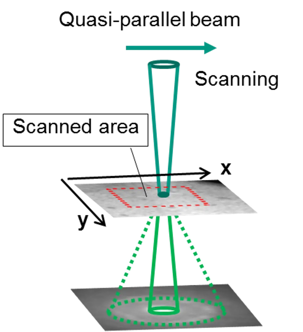
The JEOL JEM-2100F S/TEM has been retrofitted with a NanoMEGAS TOPSPIN beam precession platform. Using this system, the electron beam can be rotated/precessed at a tilted incident angle to the optic axis of the TEM. Quasi-kinematical electron diffraction patterns – more amenable to automated determination of crystal structure – can be collected by integrating the patterns collected as the beam is precessed.
This can actually be taken a step further, and by recording such a pattern at each pixel in an image, the crystal orientation and phase can be spatially mapped in that region, down to the nanoscale. These patterns can be automated identified and indexed against a database of known patterns using the NanoMEGAS ASTAR tool to create phase and orientation maps to help better understand material texture at the micro- to nano-scale.
For more details about this capability (plus examples), see the NanoMEGAS site.
08: Quantitative Mass Measurement (Quantitative STEM)
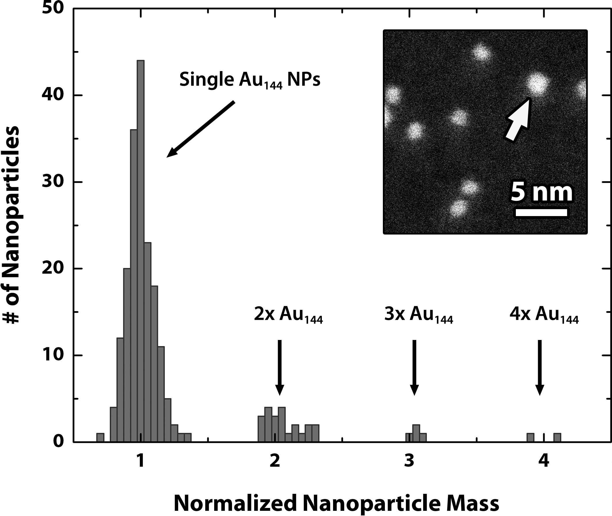
Quantitative STEM is a family of techniques where the intensity of a nanoparticle or atomic column in an image can be directly related back to the number of atoms in that particle or column. The former is particularly useful for gauging the monodispersity of a nanoparticle sample, since the mass is more sensitive to deviation than the diameter is. At Pitt, we have developed a methodology and the accompanying analysis software for rapidly performing this analysis on statistically robust particle populations1.
This capability is currently available on the JEOL JEM-2100F and the FEI Themis G2 200.
1.S.D. House et al., Ultramicroscopy, 2017, 182, pp. 145-155.
Figure: Quantitative STEM revealed that the observed larger nanoparticles (arrow) were actually coalesced integer multiples of Au144(SR)60 nanoparticles1.
09: Surface Topography (SEM)
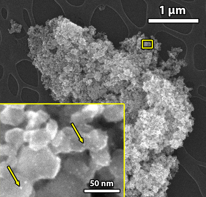
Scanning electron microscopes (SEM) are low-voltage microscopes that collect secondary and backscattered electrons, rather than high-energy transmitted electrons as in TEM. This enables just the surfaces of materials (and near-surfaces) to be imaged. Example applications for catalysis include determining whether and where catalyst nanoparticles are residing on the support structures, or imaging the surface topography of thin-film substrates.
The Zeiss Sigma 500 SEM is capable of 1 nm spatial resolution.
Figure: Small Pd nanoparticles (e.g., arrows) on TiO2 support catalyst system.
10: Ex situ Gas Reactor
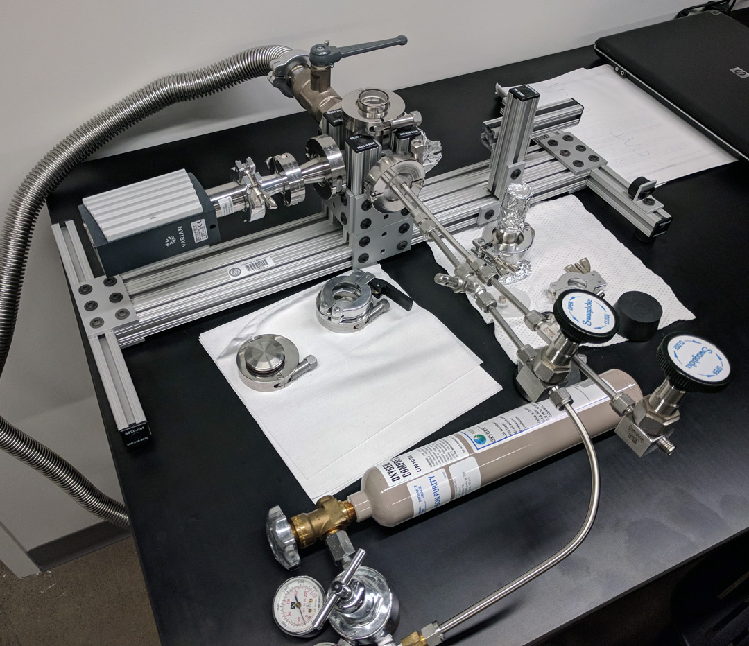
This custom-built ex situ reactor allows the reaction of TEM samples at up to 1 atm of gas pressure and temperatures up to 900 °C. It is compatible with the TEM holders, enabling the same specimens to be used both for ex situ gas reaction and before/after TEM examination.
1: Hitachi H-9500 Environmental TEM
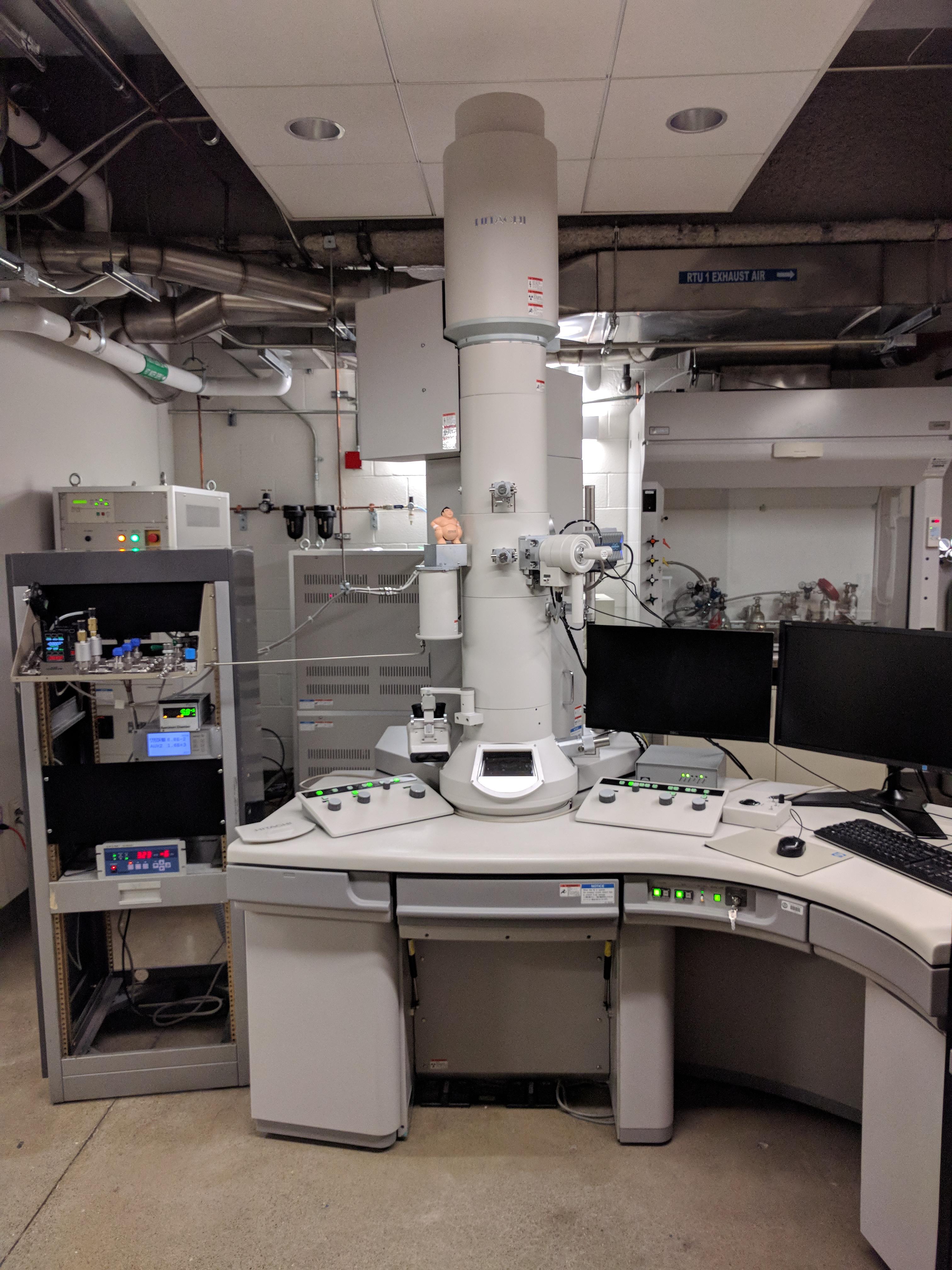
The Hitachi H-9500 ETEM is a dedicated high-resolution 100-300 keV TEM specifically designed for performing in situ reactions in gaseous environments. A computer-controllable gas manifold system allows for creation of atmospheres consisting of mixtures of up to 2 gases and 1 vapor. A fume hood has been integrated into the gas-handling setup to expand the range of gases that can be incorporated. Currently attached gas sources include H2, O2, CO, CO2, CH3OH, and CH4; this selection can be easily expanded. Two specialized sample holders enable heating of a wide variety of samples up to 900 °C with or without gas. A double-tilt furnace-style holder accepts standard 3 mm TEM specimens, and a Protochips Aduro holder uses MEMS-style heating chips. Specimens can be examined in liquid environments using a specialized liquid flow-cell sample holder. The microscope is also equipped with an energy-dispersive X-ray spectrometer (EDXS) for elemental composition determination.
2: FEI Titan Themis G2 200, AC-STEM/TEM
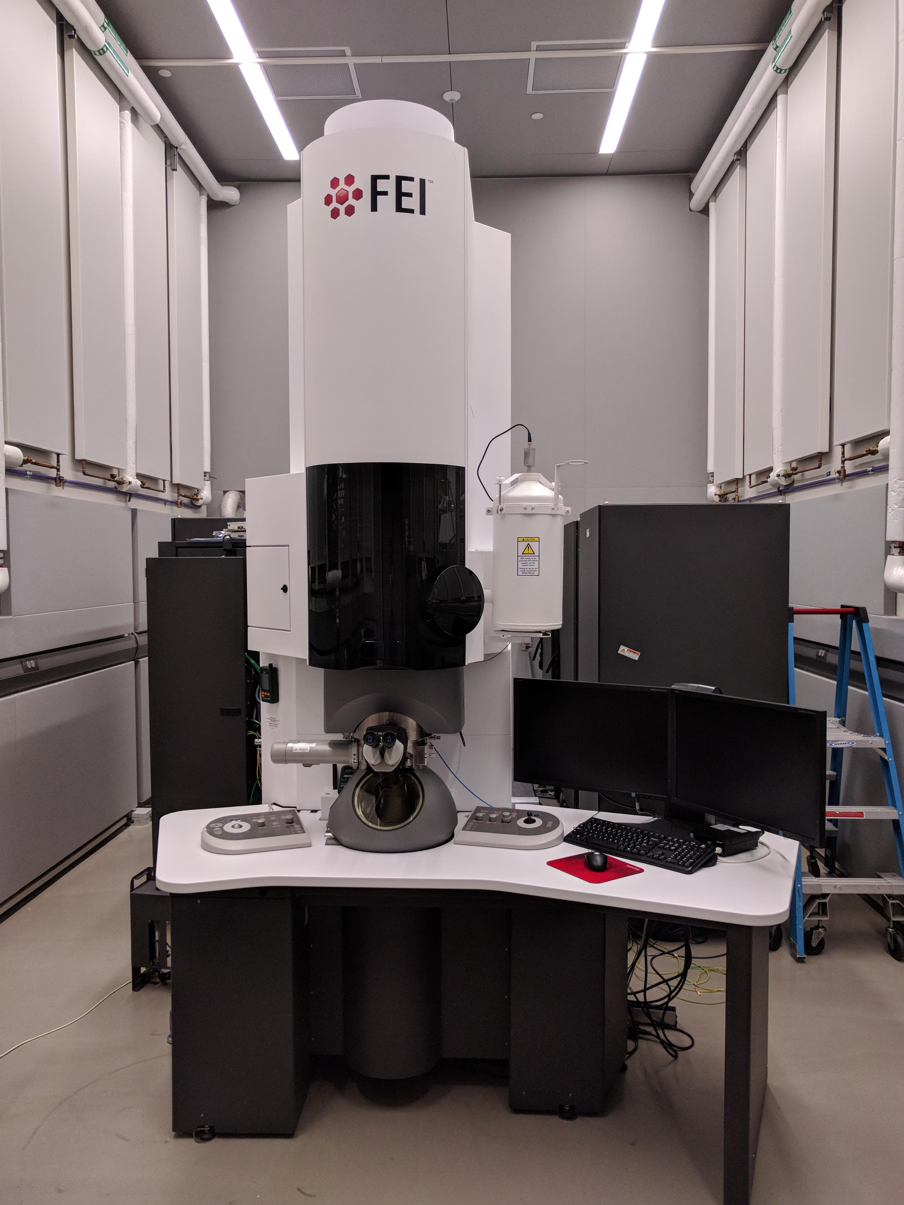
The FEI Titan Themis G2 200 TEM/STEM is an 80-200 keV probe aberration-corrected microscope, enabling true atomic-resolution (sub-Å) STEM imaging and spectroscopy. The high-brightness X-FEG electron source and Super-X quad-EDXS (0.7 sr) detector provide high-speed, high-sensitivity image and spectrum acquisition, making it possible to quantitatively spatially map the elemental distributions within nanoparticles below 2 nm. The microscope is also specifically designed for electron and EDXS tomography, which can reconstruct true three-dimensional models of the structure and elemental distribution of nanostructures. The Themis can also be configured for low-dose conditions, useful for minimizing damage in beam-sensitive specimens, such as certain oxides or nanoparticle systems.
3: JEOL JEM-2100F TEM/STEM
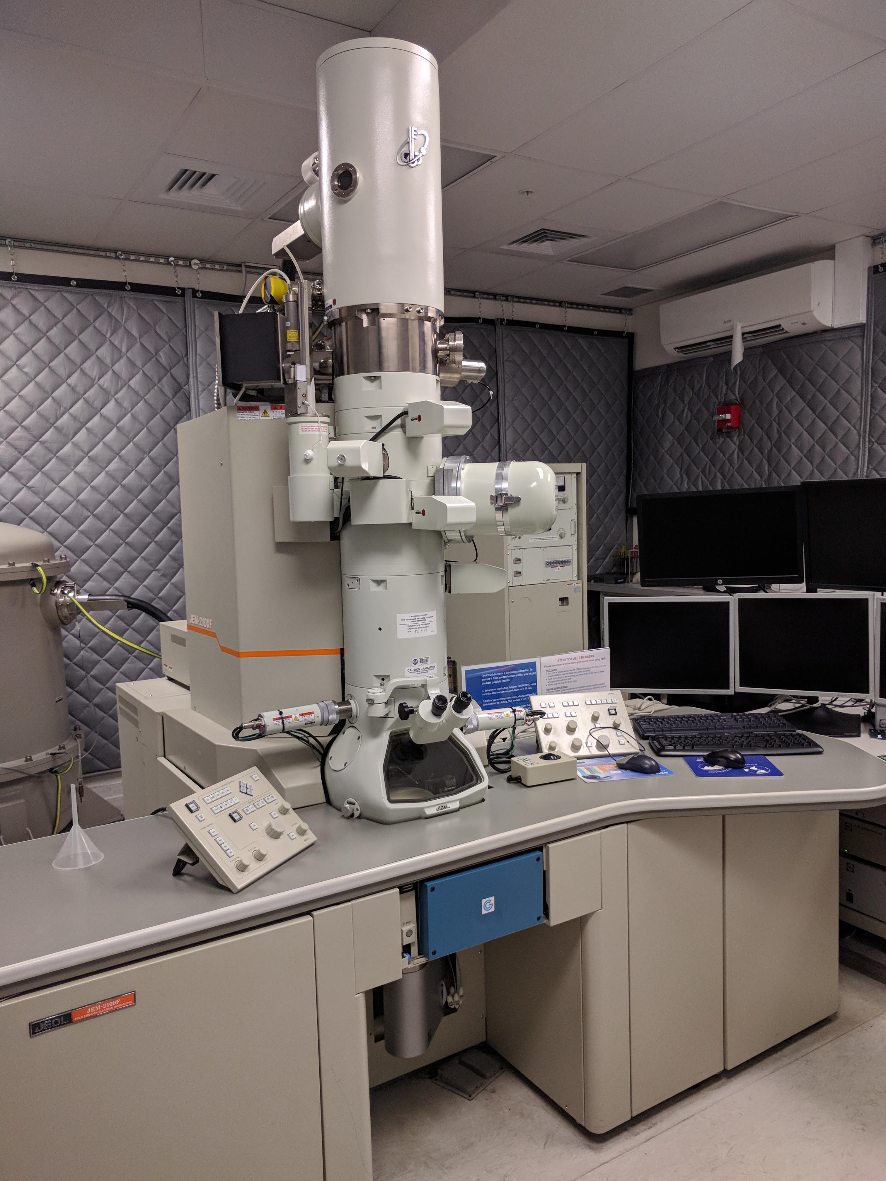
The JEOL JEM-2100F is a 120-200 keV analytical TEM/STEM capable of a wide range of imaging, diffraction, and spectroscopy modes. This includes atomic-resolution imaging of crystal lattices (HRTEM), sub-nm Z-contrast (mass-based) STEM imaging, and both select-area and convergent-beam electron diffraction. It is equipped with an 80 mm2 Oxford X-MaxN 80 T EDXS detector for elemental analysis, a NanoMEGAS TOPSPIN system (phase and orientation mapping, etc), and a Gatan GIF Tridiem post-column energy filter for acquiring EELS spectra and energy-filtered imaging and diffraction.
4: Zeiss Sigma 500 VP Analytical FE-SEM
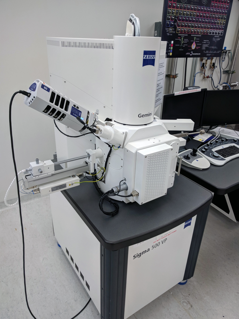
The Sigma 500 VP is a field-emission SEM that produces exceptional images at both high and low accelerating voltage, with spatial resolution up to 1 nm. Together with its analytical capabilities, this instrument is suitable for a wide range of applications in materials and life science. It is equipped with an 80 mm2 Oxford X-MaxN 80 T EDXS detector for elemental analysis, and has detectors for secondary, backscattered, and transmitted electron imaging.
Pricing
| Instrument | Rate ($/hr) | ||
|---|---|---|---|
| Internal | External Non-Profit | External Commercial | |
| Hitachi H-9500 & JEOL JEM-2100F | 55 | 115 | 150 |
| FEI Titan Themis G2 200 | 82 | 145 | 210 |
| Zeiss Sigma 500 VP | 40 | 100 | 140 |
| ECC Staff Time (Add-on) | 60 | 80 | 140 |
